|
When Organized Crime Applies Academic Results
A Forensic Analysis of an In-Card Listening Device
Houda Ferradi, Rémi Géraud, David Naccache, and Assia Tria
1
École normale supérieureComputer Science Department45 rue d’Ulm,
f
-75230 Paris
cedex 05
, FranceEmail:
given_name.family_name@ens.fr
2
CEA-TEC PACACentre Microélectronique de Provence880 Route de Mimet, 13541 Gardanne, FranceEmail:
assia.tria@cea.fr
Abstract.
This paper describes the forensic analysis of what the authors believe to be the most
sophisticated smart card fraud encountered to date. In 2010, Murdoch
et al.
[7] described a man-in-
the-middle attack against EMV cards. [7] demonstrated the attack using a general purpose FPGAboard, noting that “
miniaturization is mostly a mechanical challenge, and well within the expertise
of criminal gangs
”. This indeed happened in 2011, when about 40 sophisticated card forgeries
surfaced in the field.
These forgeries are remarkable in that they embed two chips wired top-to-tail. The first chip isclipped from a genuine stolen card. The second chip plays the role of the man-in-the-middle and
communicates directly with the point of sale (PoS) terminal. The entire assembly is embedded in
the plastic body of yet another stolen card.
The forensic analysis relied on X-ray chip imaging, side-channel analysis, protocol analysis, and
microscopic optical inspections.
1 Introduction
EMV [2
–
5] (Europay, MasterCard, Visa) is a global standard, currently managed by the public
corporation EMVCo, specifying interactions between integrated circuit cards and PoS terminals.
The standard also defines exchanges between cards and automatic teller machines (ATMs).Over the recent years, additional payment operators (such as JCB, AmericanExpress, China
UnionPay and Discover) endorsed EMV. EMV cards rely on pre-existing physical, link, network,
and transport layer protocols such as ISO/IEC 7816 and ISO/IEC 14443.
According to EMVCo’s website, by Q4 2014 a third of card present transactions worldwide
followed the EMV protocol, and
3
.
423
billion EMV cards were in circulation.
1.1 Brief Overview of an EMV Transaction
A typical EMV transaction breaks down into three phases:
(1)
card authentication,
(2)
cardholder
verification and
(3)
transaction authorization.
During card authentication, the PoS explores the applications supported by the card (
e.g.
credit, debit, loyalty, ATM, etc.).
During cardholder verification, the PoS queries the PIN from the user and transmits it to the
card. The card compares the PIN and responds by “yes” (
SW
code
3
0x9000
) or “no” (
0x63CX
4
).
Transaction authorization starts by feeding the card with the transaction details
T
(
e.g.
amount, currency, date, terminal ID, fresh randomness, etc.). The card replies with an authoriza-tion request cryptogram (ARQC) based on
T
. {ARQC,
T
} is sent to the issuer
5
, who replies with
3
Whenever a command is executed by a card, the card returns two status bytes called
SW1
and
SW2
. These bytes
encode a success or a failure cause.
4
X
denotes the number of further PIN verifications remaining before lock-up.
5
For our purposes, the issuer can be thought of as the bank.

an authorization request code (ARC) instructing the PoS how the transaction should proceed.
The issuer also sends to the PoS an authorization response cryptogram (ARPC) which is a MACof {ARQC, ARC}. ARPC is transmitted to the card that responds with a transaction certificate
(TC) sent to the issuer to finalize the transaction.We refer the reader to [7] for a comprehensive diagram illustrating these three phases.
1.2 Murdoch et al.’s Attack
The protocol vulnerability described in [7] is based on the fact that the card does not condition
transaction authorization on successful cardholder verification.
Hence the attack consists in having the genuine card execute the first and last protocol
phases, while leaving the cardholder verification to a man-in-the-middle device.
To demonstrate this scenario’s feasibility, Murdoch
et al.
produced an FPGA-based proof-of-
concept, noting that miniaturisation remains a mechanical challenge.
1.3 Fraud in the Field
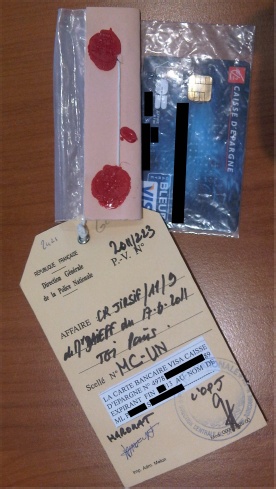
Fig.1.
The judicial seizure. Personal information such as cardholder name are censored for privacy reasons.
In May 2011, the French’s bankers Economic Interest Group (GIE Cartes Bancaires) notedthat a dozen EMV cards, stolen in France a few months before, were being used in Belgium. A
police investigation was thus triggered.2
Because transactions take place at well-defined geographic locations and at well-defined
moments in time, intersecting the IMSIs
6
of SIM cards present near the crime scenes immediately
revealed the perpetrators’ SIM card details. A 25 years old woman was subsequently identifiedand arrested, while carrying a large number of cigarette packs and scratch games. Such larceny
was the fraudsters’ main target, as they resold these goods on the black market.
Investigators quickly put a name on most of the gang members. Four were arrested, including
the engineer who created the fake cards. Arrests occurred in the French cities of Ezanville,
Auchy-les-Mines and Rouvroy. About 25 stolen cards were seized, as well as specialized software
and
e
5000 in cash.
The net loss caused by this fraud is estimated to stand below
e
600,000, stolen over 7,000
transactions using 40 modified cards.A forensic investigation was hence ordered by Justice [1].
2 Physical Analysis
2.1 Optical Inspection
The forgery appears as an ISO/IEC 7816 smart card. The forgery’s plastic body indicates thatthe card is a VISA card issued by Caisse d’Épargne (a French bank). The embossed details are:PAN
7
=
4978***********89
; expiry date in 2013
8
; and a cardholder name, hereafter abridged
as P.S. The forgery’s backside shows a normally looking CVV
9
. Indeed, this PAN corresponds to
a Caisse d’Épargne VISA card.
The backside is deformed around the chip area (Figure 2). Such a deformation is typicallycaused by heating. Heating (around 80
◦
C) allows melting the potting glue to detach the card
module.
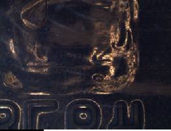
Fig.2.
Deformation due to heating of the forgery’s backside.
The module looks unusual in two ways:
(1)
it is engraved with the inscription “FUN”; and
(2)
glue traces clearly show that a foreign module was implanted to replace the
**89
card’s
original chip (Figure 3).
6
International Mobile Subscriber Identity.
7
Permanent Account Number (partially anonymized here).
8
Precise date removed for privacy reasons.
9
Card Verification Value.
3
|
